Navigating ASML's Lithography Roadmap: From DUV to Hyper-NA and the Future of Chip Fabrication
Overview
ASML holds a near-monopoly on advanced lithography systems essential for manufacturing cutting-edge semiconductors. In 2025, the company shipped 48 extreme ultraviolet (EUV) lithography tools and 131 immersion deep ultraviolet (DUV) systems, generating €32.7 billion in total revenue and ending the year with a €38.8 billion order backlog. This guide unpacks ASML’s technology roadmap—from workhorse DUV scanners to the latest High-NA EUV, and the emerging Hyper-NA platform—so you can understand how each generation enables smaller, faster, and more power-efficient chips.

Whether you’re a hardware engineer, a semiconductor investor, or simply curious about the backbone of modern electronics, this tutorial will equip you with the critical knowledge to follow ASML’s progress and the broader industry trends.
Prerequisites
Before diving into the roadmap, you should be comfortable with:
- Basic semiconductor physics – understand concepts like transistors, nodes (e.g., 7nm, 5nm), and Moore’s Law.
- Lithography fundamentals – photoresist, masks, exposure, and resolution limits (Rayleigh criterion).
- Industry context – awareness of major chipmakers like TSMC, Intel, and Samsung, and their reliance on ASML equipment.
No prior experience with ASML’s specific tool models is required; we’ll introduce them step by step.
Step-by-Step: Understanding ASML’s Lithography Generations
1. DUV Immersion Lithography – The Workhorse (KrF, ArF, ArF Immersion)
Deep ultraviolet (DUV) lithography uses excimer lasers with wavelengths of 248nm (KrF) or 193nm (ArF). The key innovation is immersion: a layer of water between the final lens and the wafer increases the numerical aperture (NA) beyond 1.0, improving resolution. ASML’s immersion DUV tools (e.g., the NXT series) remain vital for less critical layers and older nodes. In 2025, they shipped 131 such systems, demonstrating enduring demand even as EUV scales up. These systems typically achieve feature sizes down to about 38nm half-pitch, enough for 22nm/16nm nodes and some 7nm designs using multi-patterning.
Key specifications: 193nm wavelength, NA up to 1.35, throughput ~275 wafers per hour.
2. EUV Lithography – Low-NA (0.33 NA)
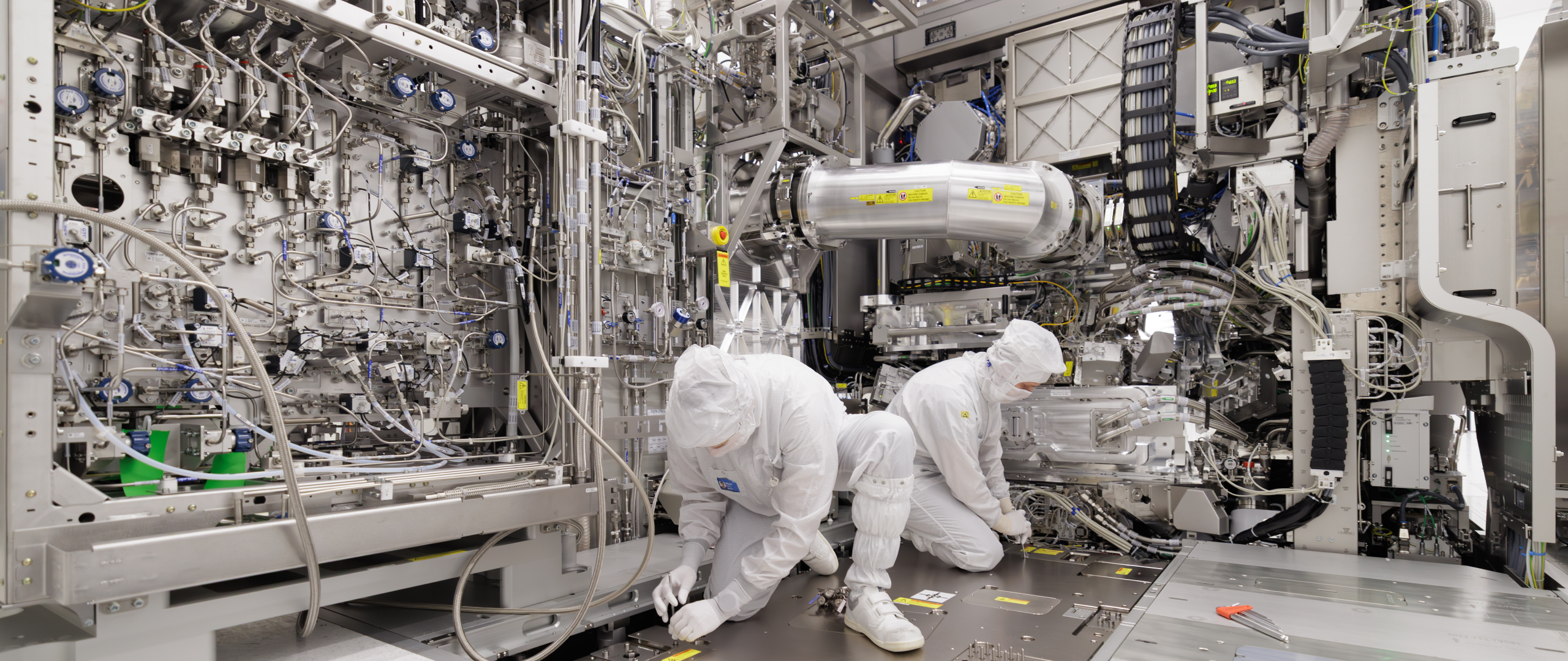
Extreme ultraviolet (EUV) systems operate at 13.5nm wavelength, drastically reducing diffraction and enabling single-exposure patterning for 7nm, 5nm, and 3nm nodes. The first generation—often called “Low-NA” EUV—uses an NA of 0.33. ASML’s NXE:3400C and NXE:3600D are examples. These tools are the backbone of modern advanced manufacturing; the 48 shipped in 2025 are valued at over €150 million each. They can resolve features down to about 13nm half-pitch, but actual production limits are around 20nm to 24nm lines due to stochastic effects and mask shadowing.
Challenges: High power (250W+ source), vacuum environment, and extremely precise reflective optics (mirrors coated with multilayer Mo/Si).
3. High-NA EUV (0.55 NA)
To continue shrinking below 3nm, ASML introduced the High-NA platform (EXE:5000 series) with a larger NA of 0.55. This allows single-exposure patterning down to about 8nm half-pitch, supporting 2nm and 1.8nm nodes. High-NA requires significant changes: larger mirrors, a new projection optics design, and a higher-power source (likely 350W+). In 2025, ASML delivered the first High-NA tools to Intel and TSMC for process development. The system's complexity and cost (over €350 million) mean adoption will be incremental.
Trade-offs: Higher resolution but smaller depth of focus, requiring better wafer flatness and more precise stage control. Throughput initially expected around 150 wafers per hour, improving over time.
4. Hyper-NA EUV – The Next Frontier
Beyond High-NA, ASML is exploring Hyper-NA with NA > 0.6, possibly reaching 0.7 or even 0.8. This would push resolution to sub-5nm half-pitch, enabling single-digit nodes (e.g., 1nm, 0.7nm). The technical hurdles are immense: new mirror coatings (perhaps using higher reflectivity multilayers like La/B4C), extreme source power (500W+), and handling of photoresist outgassing and contamination. Hyper-NA is not expected before 2030 and may require a fundamental shift in source technology (e.g., laser-induced plasma brightness improvements).
Economic implications: Each Hyper-NA tool could cost over €500 million, limiting adoption to a few high-volume manufacturers. However, for those who can afford it, Hyper-NA could extend Moore’s Law well into the next decade.
5. Beyond EUV – Alternative Approaches
ASML and its partners are also researching next-generation lithography methods:
- Multi-beam maskless lithography – e-beam direct-write for small-volume or prototyping, not high-volume production.
- Nanoimprint lithography – Canopus and other companies, but ASML sees limited scalability.
- Directed self-assembly (DSA) – using block copolymers to create patterns, often combined with EUV.
For now, ASML’s roadmap focuses on evolving EUV through NA scaling, with Hyper-NA as the primary candidate for 2030+.
Common Mistakes
When studying ASML’s roadmap, avoid these misconceptions:
- Assuming DUV is obsolete. Many layers in advanced chips still use immersion DUV due to cost and throughput. EUV is reserved for critical layers.
- Ignoring the mask infrastructure. High-NA and Hyper-NA require new mask blanks and pellicle materials – a supply chain challenge often overlooked.
- Overlooking the source power bottleneck. Without sufficient photon flux, throughput drops. Progress depends on laser power and collector mirror lifetime.
- Confusing NA with resolution. NA is just one factor; resolution also depends on wavelength (fixed for EUV) and process constant (k1).
Summary
ASML’s lithography roadmap is a multi-generational journey: from DUV immersion (still a cash cow), through Low-NA and High-NA EUV, toward Hyper-NA and beyond. In 2025, the company’s 48 EUV and 131 immersion DUV shipments underscore the sustained demand for both mature and cutting-edge tools. As chipmakers race to sub-2nm nodes, understanding these technology generations—their capabilities, costs, and limitations—is essential for anyone tracking the semiconductor industry.
Key takeaway: ASML controls the printing press for the digital age, and its roadmap will determine whether Moore’s Law continues to run its course or begins to slow.